Research
~ Nanoelectronics
~ Semiconductor Devices
~ Semiconductor Technology
~ Intelligent sensor devices for environmental monitoring and healthcare

Synthesis of 2D Materials
Synthesis techniques: CVD, PVD, and wet chemical process
Thermal CVD process is mainly used for the growth of 2D TMDCs materials (MoS2, WS2, SnS2, etc.).
The wet-chemical processes are used for exfoliation, and synthesis of MXenes, and various nanostructures (nanowires, nanorod, micro flowers, etc.) of the materials.

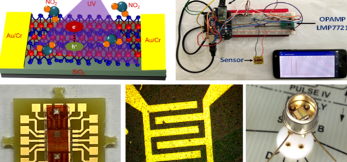
Chemical Sensors
Semiconductor Sensors: Resistive and FET
Machine learning-assisted development of electronic nose (E-nose) for breath-based point of care diagnostics.
Sensors are employed for the detection of toxic and hazardous gases such as NOx, COx, H2, H2S, SO2, etc.
Sensors are also developed for healthcare applications through the detection of VOCs and humidity.

Photodetectors
Semiconductor Photodetector: UV, Visible and IR ranges
Photodetectors are fabricated using 2D materials (Graphene, MoS2, WS2, etc.) or III-V direct bandgap semiconductors and van der Waals heterostructures.

Pressure Sensors
Flexible and bio-degradable wearable devices
Wearable pressure sensors are fabricated using paper, fabric, sponge, etc. for applications in Artificial skin, Human-machine interfacing, IOTs, health-care and electronic applications, etc.

Heterostructures
Mixed-dimensional heterojunctions such as 2D/3D, 2D/2D, 2D/1D, 2D/0D etc.
Visualization of band alignment for designed heterostructures to get a deeper understanding of carrier dynamics at the heterointerface.
Different mixed-dimensional heterostructures are exploited in the development of advanced electronic sensors.
